- 您现在的位置:买卖IC网 > Sheet目录322 > DS1345YP-70IND+ (Maxim Integrated Products)IC NVSRAM 1MBIT 70NS 34PCM
�� �
�
�DS1345Y/AB�
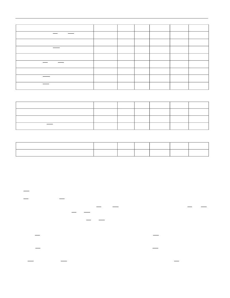
�POWER-DOWN/POWER-UP� TIMING�
�(T� A� :� See� Note� 10)�
�PARAMETER�
�V� CC� Fail� Detect� to� CE� and� WE� Inactive�
�SYMBOL�
�t� PD�
�MIN�
�TYP�
�MAX�
�1.5�
�UNITS�
�μ� s�
�NOTES�
�11�
�V� CC� slew� from� V� TP� to� 0V�
�t� F�
�150�
�μ� s�
�V� CC� Fail� Detect� to� RST� Active�
�V� CC� slew� from� 0V� to� V� TP�
�V� CC� Valid� to� CE� and� WE� Inactive�
�V� CC� Valid� to� End� of� Write� Protection�
�t� RPD�
�t� R�
�t� PU�
�t� REC�
�150�
�15�
�2�
�125�
�μ� s�
�μ� s�
�ms�
�ms�
�14�
�V� CC� Valid� to� RST� Inactive�
�V� CC� Valid� to� BW� Valid�
�t� RPU�
�t� BPU�
�150�
�200�
�350�
�1�
�ms�
�s�
�14�
�14�
�BATTERY� WARNING� TIMING�
�(T� A� :� See� Note� 10)�
�PARAMETER�
�SYMBOL�
�MIN�
�TYP�
�MAX�
�UNITS�
�NOTES�
�Battery� Test� Cycle�
�Battery� Test� Pulse� Width�
�Battery� Test� to� BW� Active�
�t� BTC�
�t� BTPW�
�t� BW�
�24�
�1�
�1�
�hr�
�s�
�s�
�(T� A� =� +25� °� C)�
�PARAMETER�
�Expected� Data� Retention� Time�
�SYMBOL�
�t� DR�
�MIN�
�10�
�TYP�
�MAX�
�UNITS�
�years�
�NOTES�
�9�
�WARNING:�
�Under� no� circumstance� are� negative� undershoots,� of� any� amplitude,� allowed� when� device� is� in� battery�
�backup� mode.�
�NOTES:�
�1.� WE� is� high� for� a� Read� Cycle.�
�2.� OE� =� V� IH� or� V� IL� .� If� OE� =� V� IH� during� write� cycle,� the� output� buffers� remain� in� a� high-impedance� state.�
�3.� t� WP� is� specified� as� the� logical� AND� of� CE� and� WE� .� t� WP� is� measured� from� the� latter� of� CE� or� WE�
�going� low� to� the� earlier� of� CE� or� WE� going� high.�
�4.� t� DS� is� measured� from� the� earlier� of� CE� or� WE� going� high.�
�5.� These� parameters� are� sampled� with� a� 5pF� load� and� are� not� 100%� tested.�
�6.� If� the� CE� low� transition� occurs� simultaneously� with� or� latter� than� the� WE� low� transition,� the� output�
�buffers� remain� in� a� high-impedance� state� during� this� period.�
�7.� If� the� CE� high� transition� occurs� prior� to� or� simultaneously� with� the� WE� high� transition,� the� output�
�buffers� remain� in� high-impedance� state� during� this� period.�
�8.� If� WE� is� low� or� the� WE� low� transition� occurs� prior� to� or� simultaneously� with� the� CE� low� transition,�
�the� output� buffers� remain� in� a� high� impedance� state� during� this� period.�
�8� of� 10�
�发布紧急采购,3分钟左右您将得到回复。
相关PDF资料
DS1350WP-100IND+
IC NVSRAM 4MBIT 100NS 34PCM
DS1350YP-70IND+
IC NVSRAM 4MBIT 70NS 34PCM
DS1609-50+
IC SRAM 2KBIT 50NS 24DIP
DS2016R-100+
IC SRAM 16KBIT 100NS 24SOIC
DS2030L-100#
IC NVSRAM 256KBIT 100NS 256BGA
DS2030W-100#
IC NVSRAM 256KBIT 100NS 256BGA
DS2030Y-70#
IC NVSRAM 256KBIT 70NS 256BGA
DS2045L-100#
IC NVSRAM 1MBIT 100NS 256BGA
相关代理商/技术参数
DS1345YP-C01
功能描述:NVRAM 1024K NV SRAM w/Battery Monitor RoHS:否 制造商:Maxim Integrated 数据总线宽度:8 bit 存储容量:1024 Kbit 组织:128 K x 8 接口类型:Parallel 访问时间:70 ns 电源电压-最大:5.5 V 电源电压-最小:4.5 V 工作电流:85 mA 最大工作温度:+ 70 C 最小工作温度:0 C 封装 / 箱体:EDIP 封装:Tube
DS1346
制造商:MAXIM 制造商全称:Maxim Integrated Products 功能描述:Low-Current, SPI-Compatible Real-Time Clocks
DS1346T+
功能描述:实时时钟 Low Power SPI RTC For 6Pf Crystal RoHS:否 制造商:Microchip Technology 功能:Clock, Calendar. Alarm RTC 总线接口:I2C 日期格式:DW:DM:M:Y 时间格式:HH:MM:SS RTC 存储容量:64 B 电源电压-最大:5.5 V 电源电压-最小:1.8 V 最大工作温度:+ 85 C 最小工作温度: 安装风格:Through Hole 封装 / 箱体:PDIP-8 封装:Tube
DS1346T+T&R
制造商:Maxim Integrated Products 功能描述:LOW POWER SPI RTC FOR 6PF CRYSTAL - Tape and Reel
DS1346T+T&R
功能描述:实时时钟 Low Power SPI RTC For 6Pf Crystal RoHS:否 制造商:Microchip Technology 功能:Clock, Calendar. Alarm RTC 总线接口:I2C 日期格式:DW:DM:M:Y 时间格式:HH:MM:SS RTC 存储容量:64 B 电源电压-最大:5.5 V 电源电压-最小:1.8 V 最大工作温度:+ 85 C 最小工作温度: 安装风格:Through Hole 封装 / 箱体:PDIP-8 封装:Tube
DS1347
制造商:MAXIM 制造商全称:Maxim Integrated Products 功能描述:Low-Current, SPI-Compatible Real-Time Clock
DS1347_1202
制造商:MAXIM 制造商全称:Maxim Integrated Products 功能描述:Low-Current, SPI-Compatible Real-Time Clock
DS1347_13
制造商:MAXIM 制造商全称:Maxim Integrated Products 功能描述:Low-Current, SPI-Compatible Real-Time Clock